301 - Bus architectures
A SoC consists of more components than only a processor, as the name already implies. The system has multiple components depending on the task for which it was designed. Having multiple components like timers, interrupt controllers, or communication cores are very useful, unless they can’t be used. To achieve reachability, all the components must be connected through some bus architecture to the processor.
A number of standardised bus architectures exist, for example:
- Wishbone
- Avalon
- AMBA
- CoreConnect
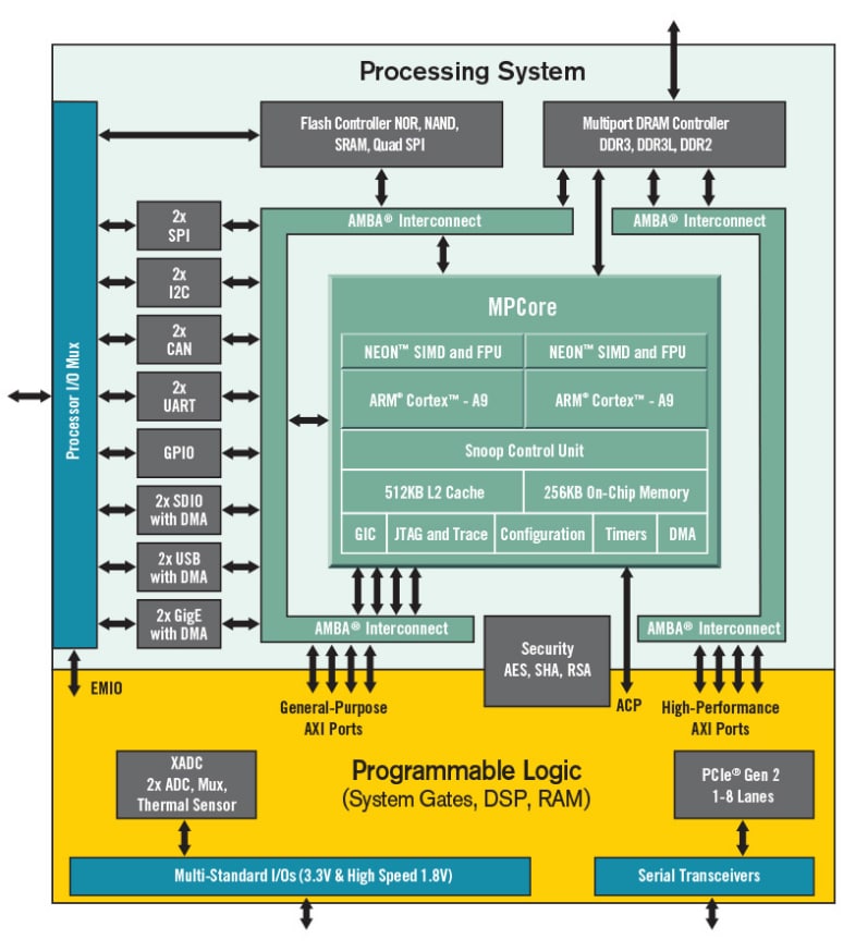
AMBA
ARM has defined an open standard which allows the interconnection of such functional blocks: Advanced Microcontroller Bus Architecture (AMBA). Currently the fifth generation of the AMBA bus is available.

image source: https://developer.arm.com/architectures/system-architectures/amba
It should not come as a surprise that the more recent versions are more powerful than the older ones, but they are also more complicated 😃. When working with design software like Xilinx’s Vivado, almost all components have an AXI4 interface. As the provided cores in such an ecosystem are all tuned towards a single standard, it becomes fairly easy for the designer to build a SoC. Two examples of how to use these buses in a system are shown in the images below.
To protect ourselves from getting lost in details, only the APB bus will be used in this course. The most recent specification of this protocol can be obtained from the ARM website.
Advanced Peripheral Bus (APB)
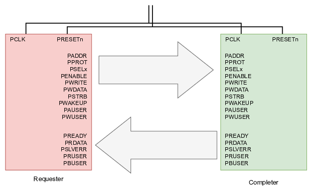
When two components are talking, typically the names master and slave are used. The lingo in the APB-bus uses: the requester and the completer. The image below shows a setup with one requester and one completer. The clock and reset signals are provided externally. Most of the signals are driven by the requester, but (offcourse) a couple of signals are driven by the completer.
For a more in-depth description of each of these signals, you can visit the specification.
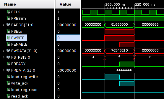
Transfers on the APB-bus follow 2 successive phases: the the setup phase and the access phase. In the setup phase the requester drives the SEL and the ADDR lines, amongst other. After one clock cycle the requester drives the ENABLE signal in the access phase.
Write transfer (without wait states)
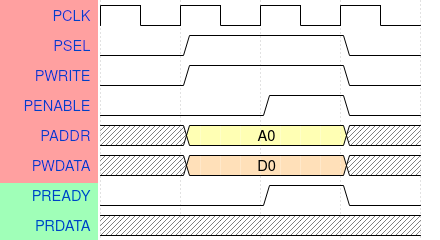
Read transfer (without wait states)
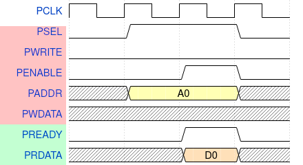
The examples above show the default write and read transfers. In the specification more detail (and explanation) is available, but putting these images right beside each other allows to better see the differences (and the similarities).
From the images and the description it is clear that each transfer takes at least two clockcycles to complete. There you have the most important reason why the bus is mainly used for peripherals.
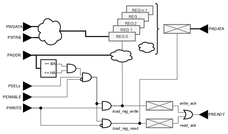
The peripherals that are connected through the APB bus typically use a register-interface. The idea behind this is that a peripheral has a number of registers that can be written and read by the processor. Based on the address map, read and write operations are handled by the targeted peripheral.
Peripheral (overhead)
Below is an example of a peripheral implementation. It contains NO functional block, but supports an APB interface.
In the top-middle part are a number registers. These can be written and read by the requester. As with many other systems, there is a strobe signal. This allows you to mask (out) the 32-bit values with byte granularity.
The register in the top-right stores the data that is to be read. This register is loaded with one of the other register OR with another value (depicted by the small cloud in the closing curly bracket).
As all the peripherals are connected through a single APB bus, every peripheral must verify if a transfer is to be obeyed or not.
This example takes into account the following conditions to determine whether or not a transfer is targeted at this peripheral:
- the address PADDR is larger than or equal to the base address (BA)
- the address PADDR is smaller than or equal to the high address (HA)
- the PSEL input is high
- the PENABLE input is low (= setup phase)
When these conditions are met, the transfer is aimed at this peripheral. Depending on the PWRITE signal, the transfer is either a write (1) or a read (0) transfer.
The transfer that is considered for this peripheral (both in case of read or write) is sampled in one of the register on the bottom right. A simple OR of these registers can be used as the PREADY signal.